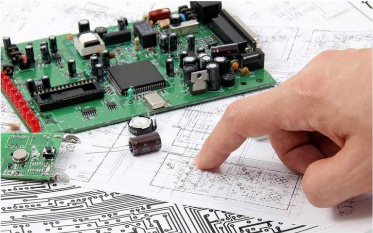
A System-on-Module can shorten development, but it does not make the carrier board an afterthought. The board determines how the processor connects to sensors, displays, storage, power sources, and external networks. A mismatch in pin assignments or power delivery can turn a promising prototype into a costly redesign.
Thoughtful circuit board design services help teams translate module capabilities into a dependable product platform. From interface mapping to thermal planning, each decision affects performance, manufacturability, and future upgrades. The goal is not simply to connect components, but to create hardware that works as a complete system.
Defining Product Requirements Before Board Architecture
A carrier board begins with the product’s purpose, operating environment, and expected interfaces. Clear requirements help engineers decide what the module must support and what belongs on the custom board.
1. Map The Interfaces To Real Use Cases
List required connections, including USB, Ethernet, display, camera, audio, storage, and wireless. Match them against the SoM’s available signals and standards. This reveals gaps before schematic work and avoids reserving space for unused interfaces.
2. Confirm Pin Availability And Multiplexing
SoM pins may serve several functions depending on processor configuration. Review multiplexing, voltage levels, boot requirements, and reserved signals before assigning functions. A clear pin map reduces peripheral conflicts and helps software teams configure hardware. Document decisions for later revisions.
3. Establish Power And Startup Requirements
Modules and peripherals may need separate voltage rails, sequencing, and current capacity. Estimate peak demand, including startup surges, standby states, and accessories. Account for protection, regulation efficiency, and possible brownouts when planning the power architecture.
4. Plan For The Physical Environment
Enclosure, mounting points, connectors, and service access influence board dimensions. Vehicles and factories may introduce vibration, dust, temperature changes, or limited airflow. Convert these conditions into requirements early to avoid late enclosure changes.
Building A Practical PCB Layout For Reliable Operation
Once the architecture is agreed, component placement and routing turn the schematic into a physical board. Layout decisions influence signal quality, power stability, thermal behavior, and assembly.
1. Arrange Components Around Signal Flow
Place the SoM connector and critical components close together to keep connections short. Keep high-speed paths controlled and avoid unnecessary layer changes. Separate sensitive analog sections from noisy switching circuits. Logical placement reduces interference and simplifies review, debugging, and manufacture.
2. Protect High-Speed Signal Integrity
DDR, PCIe, USB, Ethernet, and MIPI have demanding electrical requirements. Plan impedance, trace geometry, reference planes, and length matching as specified. Simulation can identify reflections, crosstalk, and timing concerns before fabrication. A PCB layout service should address these constraints from the initial placement stage.
3. Design Stable Power And Ground Networks
Power distribution depends on copper width, plane strategy, decoupling, and return paths. Place bypass capacitors near power pins and minimize inductive loops. Maintain signal reference planes while managing noisy currents. Power integrity analysis can reveal voltage drops and transient issues before assembly.
4. Account For Heat And Manufacturability
Processors and regulators can create concentrated heat. Review spacing, copper area, thermal vias, airflow, and heat-transfer paths. Apply design-for-manufacturing and assembly principles, including clearances, footprints, panelisation, and accessible test points for repeatable production.
Coordinating Software And Hardware During Integration
A carrier board must work seamlessly with its firmware, operating system, and mechanical structure. Coordinating these areas early helps teams prevent compatibility issues and reduce integration delays.
- Align Boot and Firmware Requirements: Confirm boot straps, reset signals, clocks, storage, and debug access with software teams. Document power-up behaviour and peripherals to support bootloader, device tree, driver, and board support package configuration.
- Verify Peripheral Compatibility: Review peripheral datasheets, voltage levels, protocols, and bandwidth before finalizing the schematic. Include level shifting, termination, or protection where required to prevent interface conflicts during hardware bring-up.
- Coordinate Mechanical and Electrical Design: Consider board outlines, connectors, antennas, shielding, and enclosure materials together. Review mounting access, cable bends, and thermal paths to resolve packaging and electrical conflicts before prototype assembly.
- Validate Designs Through Prototyping: Use prototypes to test interfaces, performance, thermal behavior, and operating conditions. Record measurable results and trace failures to the schematic, layout, components, firmware, or mechanical design before making revisions.
A coordinated integration process helps create a carrier board that performs consistently and supports smoother product development.
Validating The Carrier Board Before Production Release
Verification connects design intent with observed behaviour. A structured process gives teams evidence that the assembled product can operate consistently across its intended conditions.
1. Test Every Interface In Its Intended Mode
Test each enabled port with representative peripherals and realistic data rates. Confirm enumeration, throughput, stability, and recovery after disconnection. Include simultaneous activity where shared power or bandwidth may matter. Record conditions and results so failures can be reproduced.
2. Measure Power And Thermal Performance
Measure rail voltages, current, startup sequence, and peak-load behaviour. Monitor processor and regulator temperatures. Repeat tests inside the enclosure because open-bench airflow can hide thermal limits. Compare results with component ratings and operating requirements.
3. Review Compliance And Production Readiness
Identify relevant safety, electromagnetic compatibility, environmental, and industry requirements. Plan pre-compliance tests and address grounding, filtering, shielding, and enclosure concerns. Review component lifecycle and sourcing risks. Control production files, assembly notes, and test procedures before release.
4. Maintain Clear Revision Records
Trace each prototype change to a requirement, test result, or approved improvement. Align schematic, layout, firmware, and bill-of-materials revisions. Record limitations and configuration details for manufacturing and support teams to prevent recurring issues in later builds.
Conclusion: Advancing Product Development With Integrated Engineering
Carrier board design brings together electronics, software, mechanics, validation, and production planning to create hardware that performs reliably in real operating conditions.
For organizations seeking Embedded systems design services, Tessolve offers engineering support across hardware development, system integration, simulation, prototyping, and test validation. Their capabilities include PCB design, embedded software development, hardware integration, and System-on-Module solutions for applications across automotive, avionics, and industrial sectors. By coordinating these disciplines, they help businesses address technical requirements, improve design efficiency, and prepare products for manufacturing. Their engineering approach supports development from early concepts through hardware validation, helping teams manage integration challenges and build dependable embedded platforms.